
cy29949中文资料
7页
1、2.5V or 3.3V 200-MHz 1:15 Clock Distribution Buffer CY29949 Cypress Semiconductor Corporation3901 North First StreetSan Jose,CA 95134408-943-2600 Document #: 38-07289 Rev. *D Revised November 6, 2003 Features 2.5V or 3.3V operation 200-MHz clock support LVPECL or LVCMOS/LVTTL clock input LVCMOS-/LVTTL-compatible outputs 15 clock outputs: drive up to 30 clock lines 1X and 1/2X configurable outputs Output three-state control 350 ps max. output-to-output skew Pin compatible with MPC949, MPC9449 Ava
2、ilable in Commercial and Industrial temp. range 52-pin TQFP package Description The CY29949 is a low-voltage 200-MHz clock distribution buffer with the capability to select either a differential LVPECL or LVCMOS/LVTTL compatible input clocks. These clock sources can be used to provide for test clocks as well as the primary system clocks. All other control inputs are LVCMOS/LVTTL compatible. The 15 outputs are LVCMOS or LVTTL compatible and can drive 50 series or parallel termi- nated transmissio
3、n lines. For series terminated transmission lines, each output can drive one or two traces giving the device an effective fanout of 1:30. The CY29949 is capable of generating 1X and 1/2X signals from a 1X source. These signals are generated and retimed internally to ensure minimal skew between the 1X and 1/2X signals. SEL(A:D) inputs allow flexibility in selecting the ratio of 1X to1/2X outputs. The CY29949 outputs can also be three-stated via the MR/OE# input. When MR/OE# is set HIGH, it resets
4、 the internal flip-flops and three-states the outputs. Block Diagram Pin Configuration MR/OE# TCLK_SEL VDD TCLK0 TCLK1 PECL_CLK PECL_CLK# PCLK_SEL DSELA DSELB DSELC DSELD VSS NC VDDC QD4 VSS QD3 VDDC QD2 VSS QD1 VDDC QD0 VSS NC NC VDDC QB2 VSS QB1 VDDC QB0 VSS VSS QA1 VDDC QA0 VSS NC VSS QC0 VDDC QC1 VSS QC2 VDDC QC3 VSS VSS QD5 NC 1 2 3 4 5 6 7 8 9 10 11 12 13 39 38 37 36 35 34 33 32 31 30 29 28 27 14 15 16 17 18 19 20 21 22 23 24 25 26 52 51 50 49 48 47 46 45 44 43 42 41 40 CY29949 0 1 1 2 0 1
《cy29949中文资料》由会员小**分享,可在线阅读,更多相关《cy29949中文资料》请在金锄头文库上搜索。
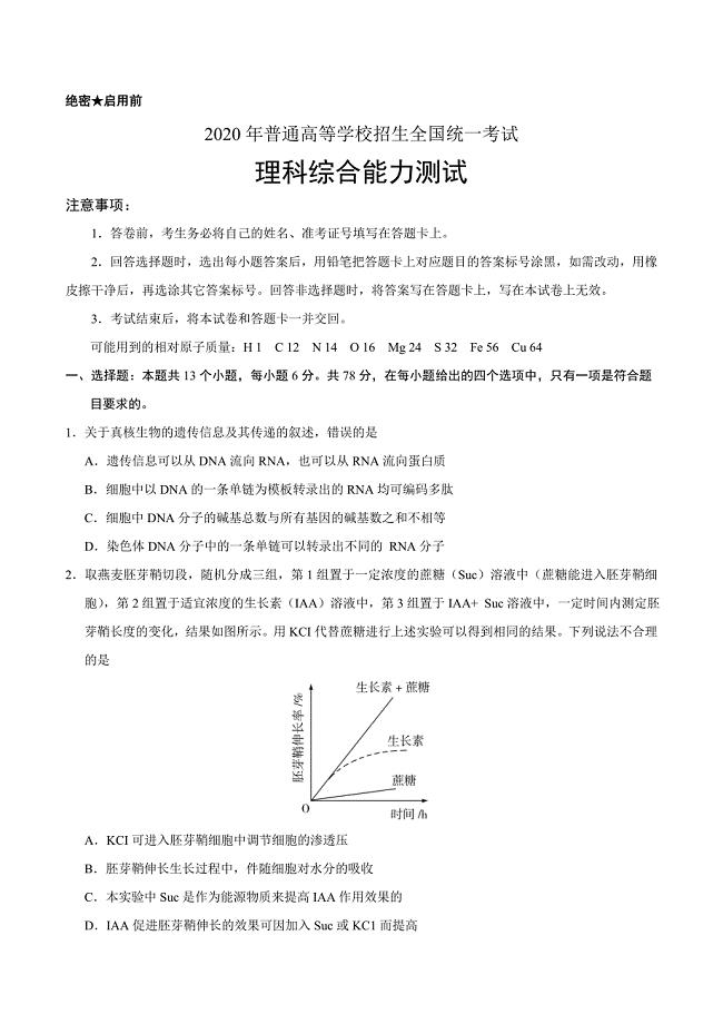
2020年高考真题——理科综合(全国卷Ⅲ)+Word版含答案
2021年绝味鸭脖策划书
2021年熟食店创业方案
2021年熟食店开店策划
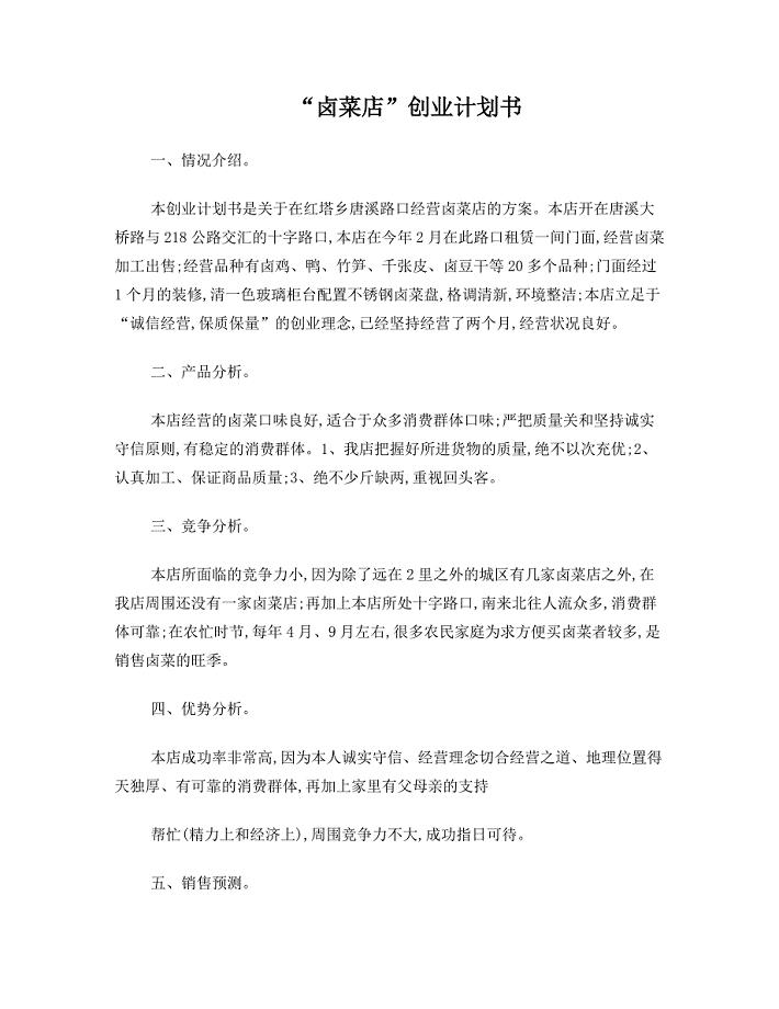
2021年卤菜店创业计划书
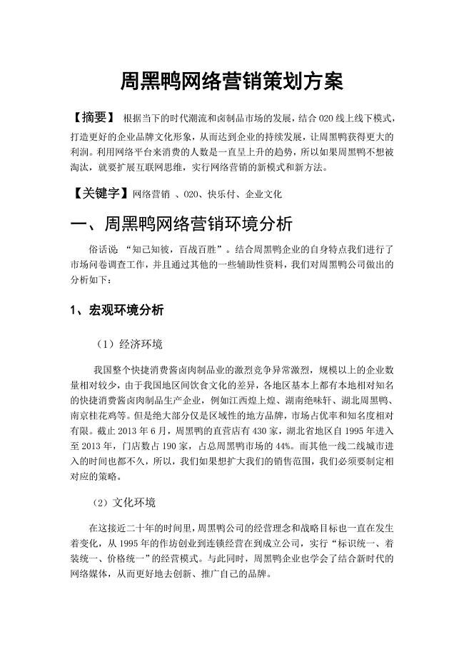
2021年周黑鸭网络营销策划方案
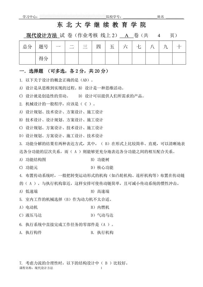
东大21年1月考试《现代设计方法》考核作业

谈我国行政管理效率的现状及其改观对策(论文)
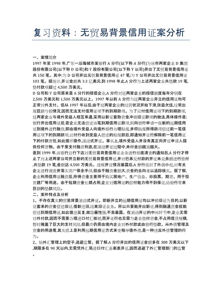
单证员考试-备考辅导-复习资料:无贸易背景信用证案分析.docx
土木工程毕业生答辩自述.docx

建筑学毕业后工作状态真实写照.doc
C#代码规范(湖南大学).doc
xx区食药监局2019年工作总结及2020年工作计划
2019年中医院药物维持治疗门诊工人先锋号先进事迹
2019年度xx乡镇林长制工作总结
2019年性艾科工作计划书
2019年人才服务局全国扶贫日活动开展情况总结
关于组工信息选题的几点思考
摘了穷帽子 有了新模样
2019年某集团公司基层党支部书记培训班心得体会
 09.石油公司制度体系诊断及优化咨询项目
2024-04-08 33页
职工教育培训经费管理办法(规模生产制造业版)
2024-04-08 10页
08.圆通银行战略咨询项目
2024-04-08 25页
企业培训费管理实施暂行细则
2024-04-08 12页
职工教育培训经费管理办法(适合中小企业)
2024-04-08 10页
企业规章制度框架体系管理规定(2024修订版)
2024-04-08 21页
05.景宏集团全面管理提升咨询项目
2024-04-08 40页
07.玉兔食品集团供应链咨询项目
2024-04-08 34页
04.大华乳业业务战略咨询项目
2024-04-08 28页
06.德邦公司精益生产管理咨询项目
2024-04-08 28页