
测控技术与仪器专业英语 张凤登UNIT-5.Basic Semiconductor Devices
10页
1、UNIT 5 Basic Semiconductor Devices,5.1 Text Semiconductor Diode 半导体二极管,New Words semiconductor ,semikndkt n. 半导体 diode daiud n. 二极管 transistor trnsist n. 晶体管,New Words (continue) silicon silikn n. 硅 germanium d:meinim n. 锗 crystalline kristlain n. 晶体的 impurity impjurti n. 杂质 rectifier rektifai n. 整流器 rectification ,rektifikein n. 整流 triac traik n. 三端双向可控硅开关(元件) diac daik n. 二端交流开关(元件) covalent kuveilnt a. 共价的 junction dkn n. 结 adjacent deisnt a. near, next to, 临近的,毗连的 equilibrium ,i:kwilibrim n.
2、 平衡,均衡 instantaneous ,instnteinjs a. momentary,瞬间的 bias bais v. 偏置,Notes: An n-type material possesses an abundance of electrons or negative charge carriers that do not take part in covalent bonding. N型材料拥有大量的不以共价键连接的电子或负电荷载流子 。 A p-type has an excess of positive charge carriers or holes that are not influenced by covalent bonding. P型材料拥有过量的不以共价键连接的正电荷载流子或空穴。,Exercises 1. Answer the following questions. The materials between the ones that conduct electrical current easily and the ones that dont
3、conduct electrical current are semiconductors. For example, silicon, germanium. They have characteristics between those of conductors and insulators. A p-type material posses excess of positive charge carriers or holes. A diode is a pn junction. It performs the function of rectification. It is possible that, due to temperature, some electrons will cross the junction from the n-type region to the p-type region. Likewise, some holes will diffuse from the p-type region to the n-type region. After t
4、his diffusion has taken place, an electrical barrier is developed between the two regions. Thus the further movement of charge carrier is prohibited and the diode is in a state of equilibrium. The instantaneous polarity of the potential connected to each terminal of the diode determines the action performed by the diode. The polarity of the battery is used to bias the diode. Because they are attracted by the positive terminal of the battery. The continuous movement of electrons and holes makes u
《测控技术与仪器专业英语 张凤登UNIT-5.Basic Semiconductor Devices》由会员E****分享,可在线阅读,更多相关《测控技术与仪器专业英语 张凤登UNIT-5.Basic Semiconductor Devices》请在金锄头文库上搜索。
逍遥游复习 知识点整理
近现代法德关系史 高三展示课3稿

当代大学生人生信仰及追求的调查研究

长相思 纳兰性德-ppt课件
课件:危机意识 一

英语ppt演讲关于阿甘正传
发达国家基础教育改革的动向与趋势 修改版

中国民间美术 课件.ppt

生物质发电技术与系统 课程ppt 第1章 生物质发电技术现状及发展趋势 2学时 -----2016
现代信号处理思考题 含答案
执业药师继续教育 抑郁症的药物治疗 100分

小学生的成长档案模板不用修改 万能型
增订六版 现代汉语 上册 第二章文字 思考与练习答案
国家财政ppt课件
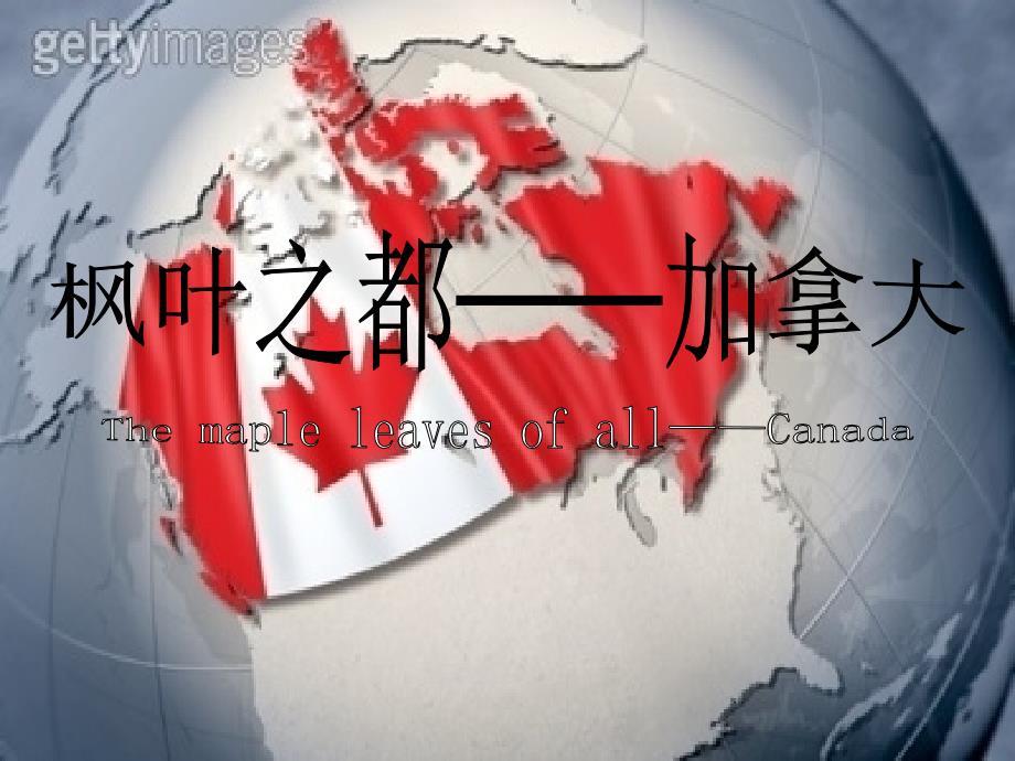
加拿大英语介绍

六年级统计图的选择课件

中学生成长档案ppt
中国现代文学史期末复习整理
lohi和hihilo训练对女子赛艇运动员运动能力影响的比较研究
风雨贾平凹阅读答案
 应对行业变革挑战策略
2024-04-11 25页
应对经济环境变化的策略布局(资料)
2024-04-11 37页
并购重组项目总结与反思
2024-04-11 28页
年度财务审计报告解读(资料)
2024-04-11 31页
年度品牌影响力报告(资料)
2024-04-11 36页
市场趋势分析与预测会议
2024-04-11 29页
市场调研报告及趋势预测(资料)
2024-04-11 22页
市场调研中的伦理与法律问题
2024-04-11 27页
市场营销趋势与消费者行为分析会议
2024-04-11 34页
市场营销扩大商业影响力
2024-04-11 32页